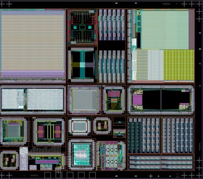
Introducing RRAM into the standard CMOS integrated circuit design flow
RRAM technology has experienced explosive growth in the next generation of nano-electronics, with multiple device structures being developed for a wide range of applications. However, this technology is only accessible to a handful of circuit designers, scientists and researchers where in-house fabrication and funds are available. Thus, transitioning the technology from the lab into the marketplace requires the development of an accessible and user-friendly design flow, supported by an industry-grade toolchain such that circuit design and validation can be done before it is laid onto the wafer and integrated with CMOS.

